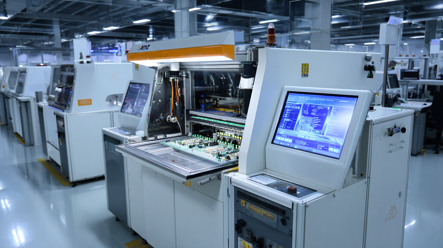
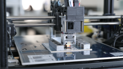
Understanding the Role of PCB X Ray Machines in Modern Electronics Manufacturing
In the rapidly evolving field of modern electronics manufacturing, the role of the PCB X Ray Machine has become increasingly prominent. As electronic devices continue to shrink in size while becoming more complex, quality assurance processes must adapt to ensure reliability and performance. According to a report by ResearchAndMarkets, the global market for X-ray inspection equipment is expected to grow significantly, projecting a compound annual growth rate (CAGR) of approximately 7.1% from 2021 to 2026. This growth underscores the importance of advanced inspection techniques, like those provided by the PCB X Ray Machine, in detecting hidden defects, ensuring proper soldering, and maintaining manufacturing standards. As manufacturers strive for higher accuracy and efficiency, the integration of PCB X Ray Machines into production lines is not just beneficial but essential for meeting evolving industry demands and safeguarding product integrity.
The Importance of PCB X-Ray Machines in Ensuring High-Quality Electronic Devices
In modern electronics manufacturing, PCB X-ray machines play a crucial role in ensuring high-quality electronic devices. These advanced inspection systems allow manufacturers to detect hidden defects within PCBs that may compromise performance and reliability.
According to a recent market analysis, the demand for semiconductor defect inspection equipment is projected to reach $3 billion by 2025, with PCB X-ray systems accounting for a significant portion of this growth due to their efficiency in identifying various defects, such as voids, solder joint integrity issues, and layer alignment problems.
The importance of PCB X-ray technology is underscored by its ability to enhance production yield and reduce costly rework. Reports indicate that manufacturers utilizing these X-ray systems have seen an improvement in their product quality assurance processes, leading to a 30% reduction in defect rates. As the complexity of electronic devices increases, the necessity for precise and reliable inspection methods becomes even more apparent, reinforcing the critical role that PCB X-ray machines play in delivering high-quality products that meet the demanding standards of today's technology-driven market.
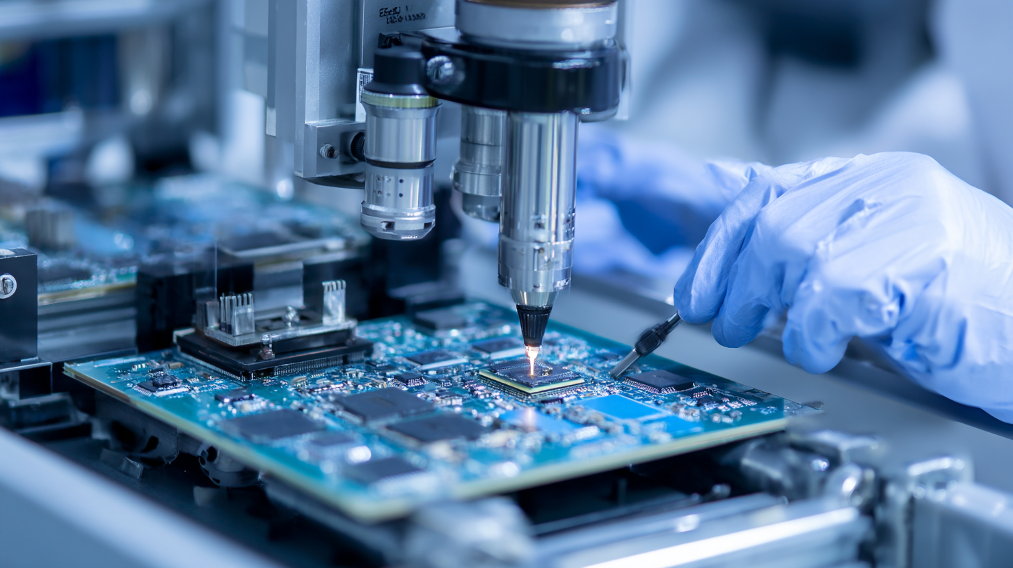
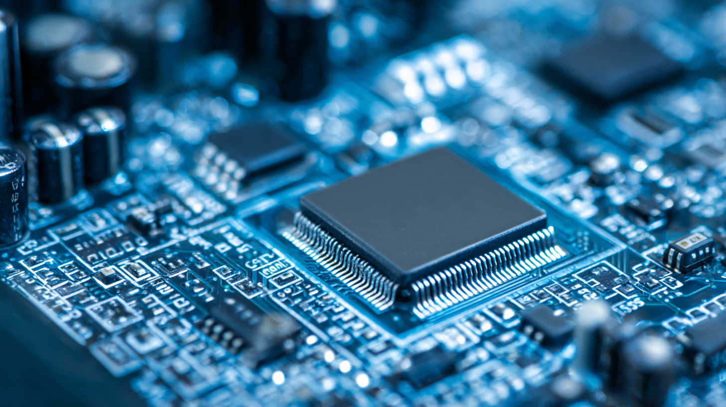
Key Features of Advanced PCB X-Ray Technology in Modern Manufacturing
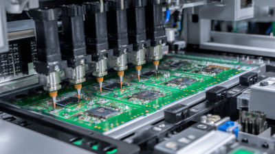
Advanced PCB X-ray technology plays a crucial role in the quality assurance of modern electronics manufacturing. One of the key features of these machines is their high-resolution imaging capability, which allows manufacturers to detect even the smallest defects in PCB assemblies. This precision is vital, as tiny errors can lead to significant failures in electronic devices. The ability to visualize the inner layers of a PCB without destructive testing streamlines the inspection process, ultimately saving time and resources.
Another important aspect is the ability to provide 3D imaging, which gives a more comprehensive view of the PCB structure. This feature enables engineers to assess the solder joints and component alignment with remarkable clarity, making it easier to identify potential issues before the product reaches the market. Additionally, advanced PCB X-ray machines are often equipped with software that can analyze and report critical data automatically, enhancing the efficiency of the manufacturing workflow and ensuring stringent quality control standards are maintained throughout the production process.
Industry Statistics: The Impact of X-Ray Inspection on PCB Failure Rates
X-ray inspection has emerged as a crucial component in modern electronics manufacturing, significantly influencing the reliability of printed circuit boards (PCBs). Industry statistics reveal that implementing X-ray machines in the inspection process has led to a remarkable decrease in PCB failure rates. For instance, manufacturers utilizing X-ray technology report failure rates dropping by up to 30%, as it identifies hidden defects such as voids, misalignments, and unrecognizable soldering issues that traditional inspection methods might overlook.
Furthermore, the integration of X-ray inspection in the manufacturing workflow enhances overall quality control, fostering consumer trust in electronic products. With the increasing complexity of electronic assemblies, the demand for precision has never been higher. Statistics indicate that companies that leverage X-ray technology not only see immediate reductions in defects but also experience long-term cost savings due to decreased warranty claims and enhanced product durability. This data underscores the transformative impact of X-ray inspection on the electronics sector, affirming its role as an indispensable tool in maintaining the integrity of modern PCBs.
Understanding the Role of PCB X Ray Machines in Modern Electronics Manufacturing
This chart illustrates the impact of X-Ray inspection on PCB failure rates across different stages of electronics manufacturing. Data shows a significant reduction in failure rates after implementing X-Ray inspection technology.
Comparative Analysis: Traditional Inspection Methods vs. PCB X-Ray Machines
In the modern electronics manufacturing landscape, the inspection of printed circuit boards (PCBs) is crucial. Traditional inspection methods, such as visual inspection and in-circuit testing (ICT), are limited in their ability to detect internal defects, which may lead to performance issues in the final product. A report by the IPC (Association Connecting Electronics Industries) highlights that visual inspection can miss up to 30% of potential faults, emphasizing the need for more advanced methodologies.
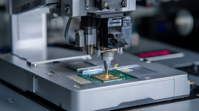
Enter PCB X-ray machines, which provide a non-destructive testing solution capable of revealing hidden defects within the layers of the PCB. According to a market research report by Frost & Sullivan, the utilization of X-ray technology in electronics manufacturing has surged, with an expected growth rate of 8.5% annually until 2025. This method allows for thorough inspections of solder joints, component placements, and internal structures, offering resolution capabilities that far exceed traditional techniques. By integrating PCB X-ray machines into their processes, manufacturers can significantly enhance product reliability and reduce the risk of costly recalls or failures in the field.
Best Practices for Implementing PCB X-Ray Systems in Manufacturing Processes
The integration of X-ray technology into PCB manufacturing has revolutionized quality assurance processes. As the complexity of electronic devices increases, the ability to accurately inspect the internal structures of printed circuit boards (PCBs) has become essential. Best practices in implementing PCB X-ray systems involve not only selecting the right equipment but also tailoring the inspection process to meet specific manufacturing needs. Industry reports indicate that effective use of X-ray systems can significantly reduce defect rates, leading to improved product reliability and customer satisfaction.
Recent advancements highlighted in discussions around industrial X-ray and CT technology emphasize the importance of innovation in this field. Advanced systems are capable of providing high-resolution imaging, which is crucial for identifying hidden defects like voids or misalignments that could compromise the performance of the final product. Studies show that manufacturers utilizing these advanced X-ray solutions report up to a 30% increase in productivity due to reduced rework and improved yield rates. This makes it clear that investing in state-of-the-art PCB X-ray machines is not just a technological upgrade, but a strategic move for companies aiming to maintain competitiveness in today's fast-paced electronics market.