Top Benefits of Selective Wave Solder in Electronics Manufacturing?
Selective Wave Solder has emerged as a transformative technology in the electronics manufacturing sector. According to a recent industry report by Market Research Future, the global selective soldering market is projected to grow at a CAGR of 5.2% from 2021 to 2027. This growth signals increasing adoption due to the benefits that selective wave soldering offers, specifically in improving efficiency and reducing defects.
Dr. Emily Carter, a respected expert in electronics assembly, emphasizes, "Selective Wave Solder allows for precision and reliability in complex assemblies." This capability is crucial as electronic products become smaller and more intricate. As manufacturers face challenges with traditional soldering methods, selective wave soldering provides a promising solution.
While it brings noteworthy advantages, the technology is not without its imperfections. For instance, initial setup costs can be high, and sourcing quality materials is essential. Additionally, operators must be well-trained to maximize the benefits of Selective Wave Solder. Building expertise in this area remains a vital hurdle for many firms. A balanced approach to these challenges will ultimately determine the success of selective wave soldering in the marketplace.
Advantages of Selective Wave Soldering in Assembly Processes
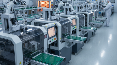
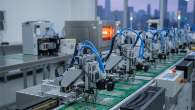
Selective wave soldering has transformed assembly processes in electronics manufacturing. This technique enables precise solder application, minimizing waste. The key advantage lies in its ability to target specific areas. By doing so, manufacturers can maintain the integrity of sensitive components. This precision also reduces the risk of solder bridging, a common issue in traditional methods.
Another notable benefit is efficiency. Selective wave soldering can handle complex designs without excessive manual intervention. This leads to faster production times. Operators can set up multiple configurations easily. However, implementing this method does require skilled personnel. Improper setup can lead to inconsistent results, which necessitates ongoing training.
Despite its advantages, there are challenges. The initial investment for selective wave soldering equipment can be high. Smaller manufacturers may find this daunting. Additionally, not all circuit designs are suited for this method. It’s essential to evaluate each project individually. In the end, selective wave soldering offers unique benefits but demands careful consideration and adaptation.
Top Benefits of Selective Wave Solder in Electronics Manufacturing
Enhanced Precision in Electronics with Selective Wave Soldering Techniques
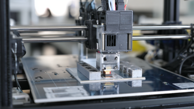
Selective wave soldering techniques have transformed electronics manufacturing by enhancing precision. This process allows for targeted solder application, minimizing waste and improving connections. Components are soldered selectively, which reduces the risk of heat damage. A well-executed selective wave soldering ensures that only the necessary areas are soldered, preserving surrounding elements.
The ability to control solder application is crucial. It creates reliable joints while maintaining the integrity of sensitive components. However, achieving the perfect balance can be challenging. Operators must be meticulous. Small adjustments in temperature or flow rate can greatly affect the final product. It's an art as much as it is a science, requiring constant reflection and fine-tuning.
Moreover, while selective wave soldering boasts many advantages, issues can arise. Sometimes, inconsistent soldering can lead to defects. Operator skill levels and machine calibration play significant roles. Even minor mistakes in settings can result in costly reworks. Continuous training and feedback are essential for improvement. Emphasizing precision is key, but acknowledging the complexity of the process is equally important.
Top Benefits of Selective Wave Solder in Electronics Manufacturing
| Benefit |
Description |
Impact on Production |
| Enhanced Precision |
Selective wave soldering allows for targeted application, reducing the risk of soldering defects. |
Increases yield and reduces waste during the manufacturing process. |
| Cost Efficiency |
Using selective soldering minimizes the amount of solder used, lowering material costs. |
Reduces overall production costs and increases profitability. |
| Reduced Thermal Stress |
Selective soldering applies heat only where needed, protecting sensitive components from damage. |
Enhances component longevity and reliability. |
| Increased Flexibility |
Allows manufacturers to work with different types of boards and components easily. |
Eases adaptation to design changes and varied production runs. |
| Improved Quality Control |
More controlled solder application leads to consistent quality across products. |
Decreases rework and increase customer satisfaction. |
Cost-Effectiveness of Selective Wave Soldering in High-Volume Production
Selective wave soldering offers significant cost-saving advantages in high-volume production. This method reduces material waste, optimizing the amount of solder used. Unlike traditional methods, it only applies solder to designated areas. This precision prevents excess solder from accumulating, which can lead to costly rework.
Labor costs also decrease with selective wave soldering. It automates soldering processes, minimizing manual interventions. However, the upfront investment in equipment can be steep. Companies must weigh this cost against potential long-term savings. Finding the right balance is crucial.
Quality control is another area for reflection. While selective wave soldering improves solder application, issues can still arise. Solder joint defects may occur if the process isn’t monitored closely. Regular equipment maintenance and calibration are essential. Achieving optimal results requires ongoing commitment and resources.
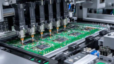
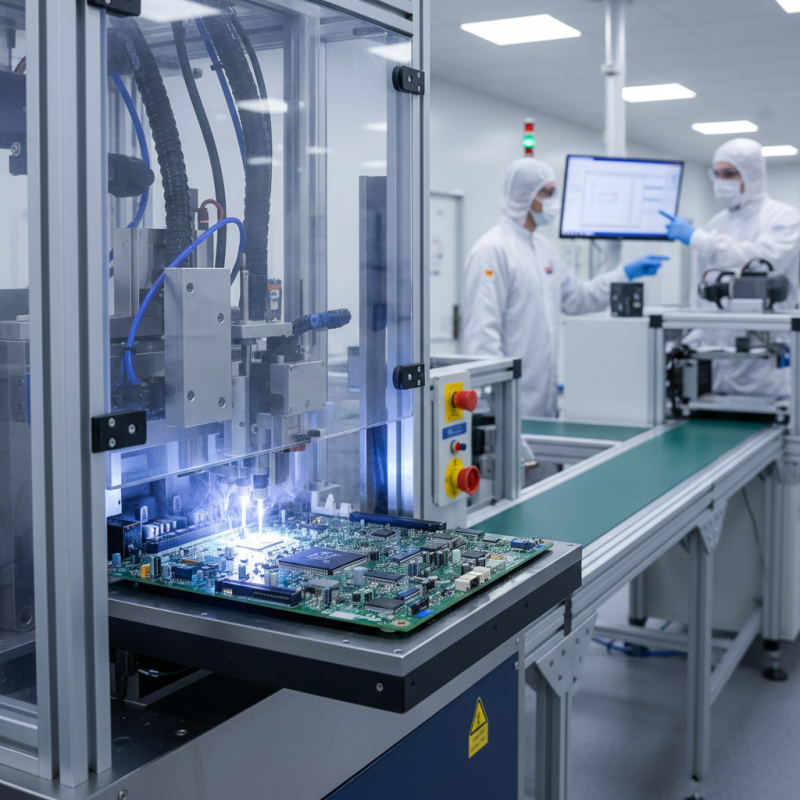
Reduction of Defects in PCB Assemblies Using Selective Wave Solder
Selective wave soldering has become a game-changer in electronics manufacturing. This method targets specific areas of a printed circuit board (PCB), applying solder only where needed. Such precision minimizes excess solder use, leading to fewer defects. In traditional methods, excess solder often bridges gaps. This can cause shorts and functional failures. With selective wave soldering, the risk of these issues decreases significantly.
Using this technique can result in improved quality control. The process provides consistent and reliable joints. Each connection receives the right amount of heat and solder. Details matter here; even slight variances can lead to performance problems. Sometimes, PCB designs contain intricate components. Selective soldering handles these complexities more effectively.
However, it’s important to recognize potential shortcomings. Training for operators is essential. Without skilled technicians, the benefits may not be fully realized. The setup process can also be lengthy, making initial implementation a challenge. Balancing these factors is key to successful adoption. Emphasizing precision can lead to mistakes in other areas if not monitored closely. Thus, continuous reflection on the process is necessary to ensure quality remains high.
Impact of Selective Wave Soldering on Production Efficiency and Speed
Selective wave soldering offers significant advantages in electronics manufacturing, particularly in enhancing production efficiency and speed. According to a study by IPC, manufacturers can achieve up to a 30% increase in throughput with selective wave soldering compared to traditional methods. This efficiency stems from the targeted application of solder to specific components, reducing unnecessary waste and time.
Furthermore, selective wave soldering minimizes cycle times. An analysis from the Electronics Manufacturing Society (EMS) reveals that companies adopting this technique see a reduction in soldering cycle time by as much as 25%. This rapid process allows for quicker adjustments and alterations during production, enabling manufacturers to meet tight deadlines without sacrificing quality.
However, there are challenges that should not be overlooked. The initial setup for selective wave soldering can be complex and requires skilled operators. Some manufacturers report that the learning curve can lead to inconsistencies in the early stages. Regular training and updates are critical to maintaining quality standards. It's essential to reflect on these aspects when considering the transition to selective wave soldering in production workflows.