Unlocking the Benefits of Selective Wave Soldering for Enhanced PCB Assembly Efficiency
In today's fast-paced electronics manufacturing landscape, enhancing PCB assembly efficiency is paramount for success. One innovative approach making waves in this realm is Selective Wave Solder, a method that offers significant advantages over traditional soldering techniques. By strategically applying solder only to specific areas of the PCB, Selective Wave Solder not only reduces material waste but also minimizes the risk of damaging sensitive components. This process optimizes thermal management, ensuring that heat-sensitive parts remain unaffected during soldering, thus improving overall reliability and performance. As manufacturers strive for greater productivity and cost-effectiveness, understanding the transformative benefits of Selective Wave Solder becomes essential. This article explores the key advantages and applications of this technology, demonstrating how it can unlock new levels of efficiency in PCB assembly.
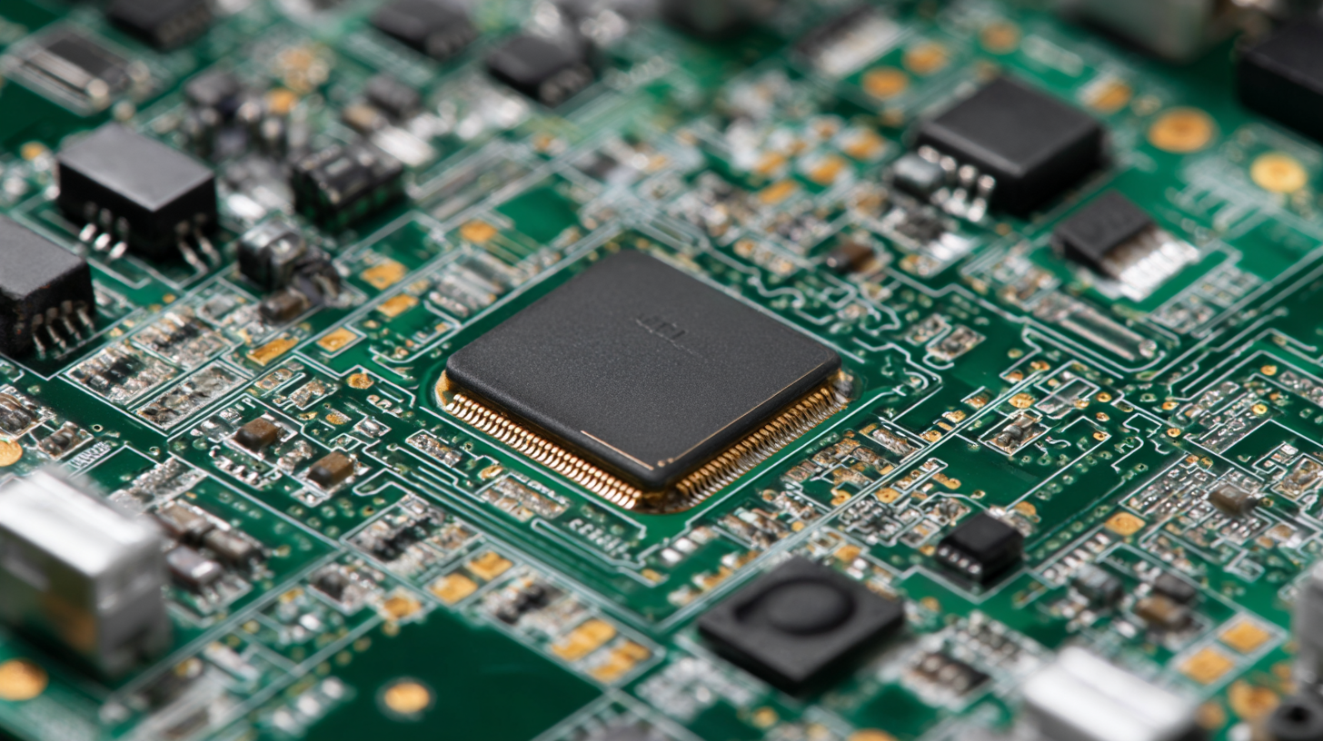
Understanding Selective Wave Soldering: Key Principles for PCB Assembly
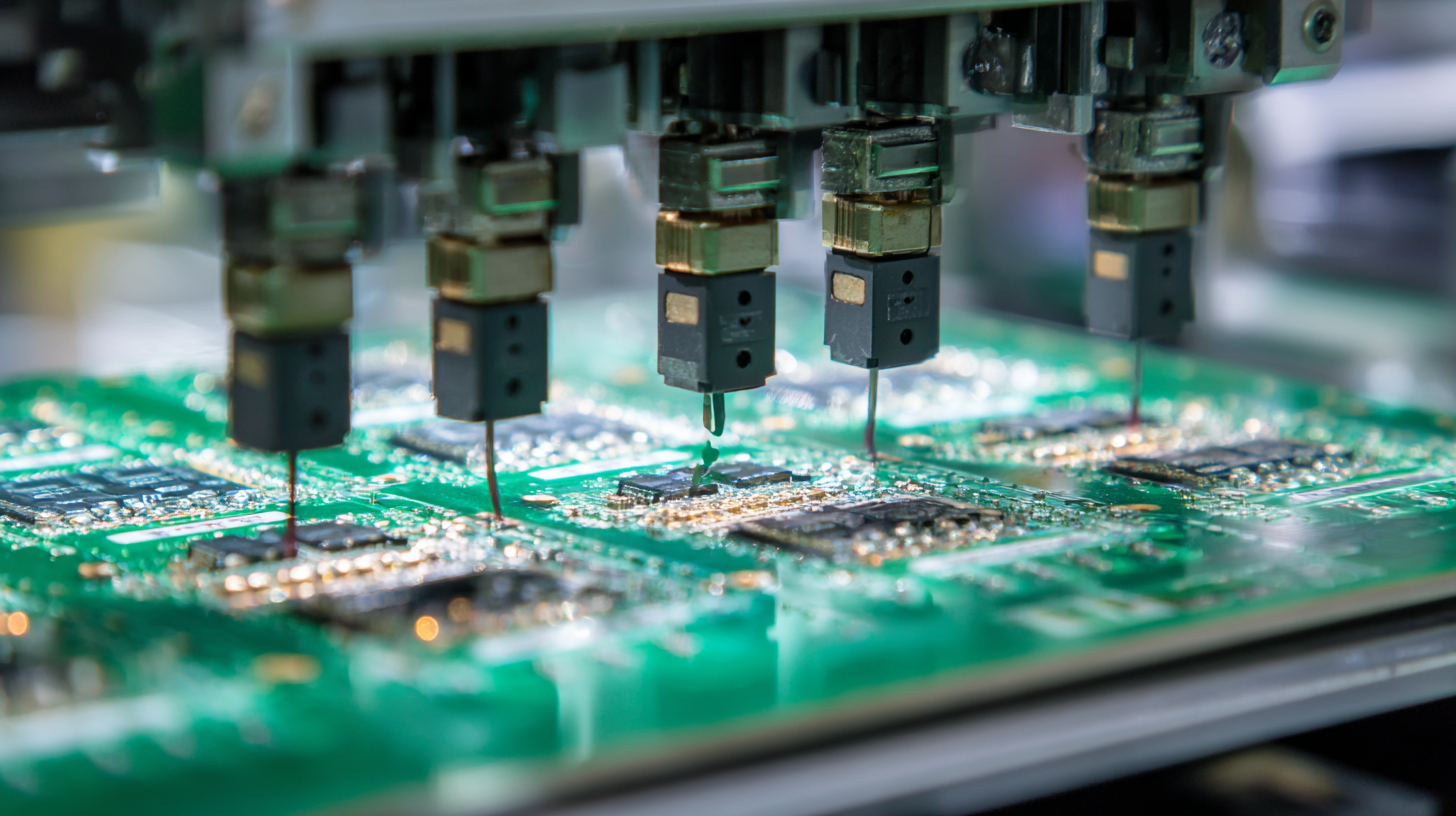
Selective wave soldering is an innovative technology that significantly enhances the efficiency of printed circuit board (PCB) assembly. At its core, this technique involves the precise application of molten solder to specific areas of a PCB, allowing for targeted soldering of components without the need for a full immersion process. By controlling the solder wave, manufacturers can minimize the risk of overheating sensitive components and reduce the likelihood of solder bridging, leading to higher quality assemblies.
Understanding the key principles of selective wave soldering is essential for optimizing its benefits. The process utilizes a specially designed solder pot that produces a controlled wave, which is directed only to the predefined areas. This targeted approach not only conserves solder but also saves time by eliminating excessive cleaning and reworking often associated with traditional methods. Additionally, selective wave soldering is highly adaptable, accommodating various board designs and component types, making it a versatile solution for modern electronics manufacturing.
Unlocking the Benefits of Selective Wave Soldering for Enhanced PCB Assembly Efficiency
| Parameter |
Description |
Value |
| Process Temperature |
Optimal soldering temperature for wave soldering |
250°C |
| Cycle Time |
Time taken to complete a soldering cycle |
30 seconds |
| Solder Alloy Composition |
Composition of the solder used |
Tin, Lead, Copper (SAC) 63/37 |
| PCB Size Compatibility |
Dimensions of compatible PCBs for selective wave soldering |
100mm x 100mm to 400mm x 400mm |
| Defect Rate |
Percentage of defects observed in solder joints |
<1% |
| Production Efficiency |
Improvement in production throughput |
20% increase |
Identifying the Advantages of Selective Wave Soldering Over Traditional Methods
Selective wave soldering has emerged as a pivotal technique in enhancing PCB assembly efficiency, particularly when compared to traditional soldering methods. One of the key advantages of selective wave soldering is its ability to minimize thermal stress on components, which can be critical in sensitive electronic assemblies. According to recent market trends, sectors incorporating selective wave soldering are witnessing a significant increase in productivity, with reports indicating a potential market growth of 7% CAGR from 2022 to 2032 in the related automated soldering equipment sector.
Another benefit of selective wave soldering lies in its precision. The method allows for targeted solder application, reducing the amount of solder used while maintaining the integrity of the connections. This is increasingly important as the electronics industry leans more toward minimizing costs and maximizing quality. As research highlights the rising demand for customized and small-batch production in electronics, selective wave soldering provides a viable solution by offering flexibility that traditional methods often cannot match. With companies actively developing solutions to address the evolving challenges in the soldering process, selective wave soldering stands out as an efficient alternative to enhance overall assembly performance and reliability.
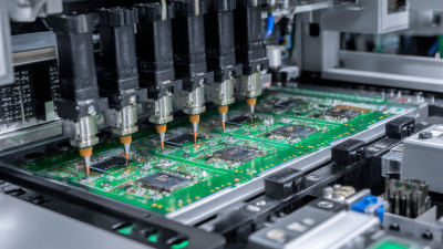
Implementing Selective Wave Soldering: Best Practices for Increased Efficiency
Selective wave soldering has emerged as a pivotal technique in enhancing PCB assembly efficiency. By focusing on specific areas of the circuit board, this method reduces the amount of solder required and minimizes thermal exposure to components that are sensitive to heat. Implementing selective wave soldering can lead to significant time savings and improved overall production timelines.
Best practices for this technique often include optimizing the heating process and selecting appropriate fluxing technologies to ensure strong solder joints. In light of recent advancements, partnerships within the industry, such as those combining expertise in equipment and fluxing technology, can further streamline the soldering process. Companies adopting these best practices can position themselves at the forefront of innovation, leveraging selective wave soldering to enhance their manufacturing capabilities and deliver higher quality products efficiently.
Unlocking the Benefits of Selective Wave Soldering for Enhanced PCB Assembly Efficiency
Maintaining Quality Control in Selective Wave Soldering Processes
Selective wave soldering is transforming PCB assembly efficiency by integrating advanced Industry 4.0 technologies such as IoT, AI, and cloud computing. These innovations enable manufacturers to interact with big data in novel ways, fostering a more refined quality control process. By optimizing the soldering process through data analytics and machine learning, companies can not only increase productivity but also minimize defects in their assemblies, thus ensuring higher reliability in electronic products.
In a recent report, it was estimated that companies using advanced analytics in manufacturing have seen a productivity increase of up to 20%. Implementing a comprehensive risk control matrix improves business processes, ensuring that any potential quality issues are addressed proactively. A streamlined workflow, combined with real-time monitoring tools, can significantly enhance operational efficiency while maintaining stringent quality standards.
**Tip:** For businesses looking to implement selective wave soldering, consider investing in advanced monitoring systems that can provide real-time data analytics. This will not only facilitate better decision-making but also enhance risk management within the production line. Another practical approach is to foster a culture of continuous improvement, where feedback loops are established to refine processes regularly, ensuring long-term success in the competitive landscape of PCB manufacturing.

Future Trends in Selective Wave Soldering for PCB Technology Advancements
The landscape of PCB technology is evolving, with selective wave soldering emerging as a pivotal process for enhancing assembly efficiency. Recent developments have shown a growing interest in leveraging this technology to meet the demands of modern electronics. With its ability to precisely target connections on PCBs, selective wave soldering minimizes waste and increases yield, making it a preferred choice for complex assembly processes. The focus on improving thermal management and reducing thermal stress is anticipated to drive further innovations in this field.
Future trends indicate an integration of advanced materials and techniques, such as frequency selective surfaces (FSS) being combined with multiple-input multiple-output (MIMO) antennas. This research highlights how such integrations could elevate performance levels in applications like the Internet of Things (IoT) and vehicle-to-vehicle (V2V) communication systems. Innovations in selective soldering equipment, along with enhanced soldering methods, are set to reshape the PCB assembly landscape, paving the way for more robust, efficient, and compact electronic solutions. As industry players invest in research and development, we can expect selective wave soldering to play a crucial role in the ongoing advancements in PCB technology.